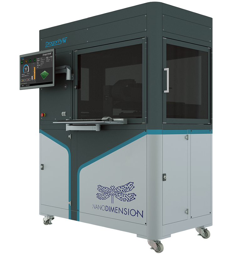
A multi-material, multi-layer 3D printer that generates entire circuits in one step including substrate, conductive traces and passive components.
Deposition Technology: Piezo drop-on-demand inkjet - Build Volume: 160mm x 160mm x 3mm - Inks:
Optimized silver nano particles and dielectric inks - Min. Dielectric Layer Thickness: 10.0 μm - Min. Conductive Layer Thickness: 1.18 μm - Supported File Formats: All major ECAD and MCAD Software, ODB++, Gerber & Excellon, STLs - Dielectric Constant (Dk): @ 2 GHz/15 GHz 2.77 / 2.78 - Tangential Loss (Df): @ 2 GHz/15 GHz 0.015 / 0.018 - Resolution: 18 µm (x), 18 µm (y), 10 µm (z) - Min. Line/Space: 75 μm traces/ 100 μm spacing - Min. BGA Pitch: 350 μm - Min. Via: 150 µm

